Inspecting an SRAM Cell
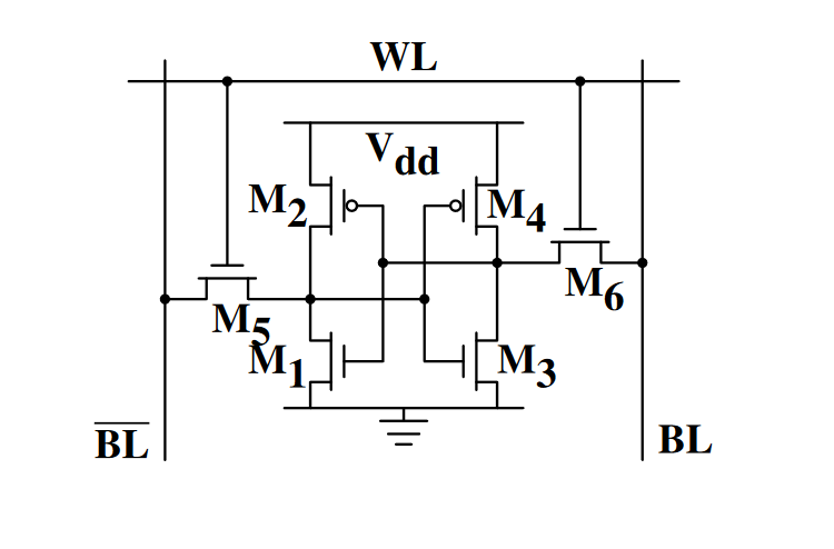
The above shows a static random access memory cell. Let's try understanding how this functions. Beginning with a brief description of the annotations:
M1 - M6: these label each of the 6 transistors
Vdd: voltage supplyy for the cell
WL: word line, allows for access to the cell for reading and writing
BL: bit line, the one with the bar on top is bit line bar. They are used to read and write data to the cell
Before analyzing the logical scenarios, here is a quick tldr on how a transistor functions. Voltage being applied to the gate affects whether current is allowed to flow from the source to the drain. There are two types of transistors being used to make up an SRAM cell - NMOS and PMOS. NMOS transistors is on when voltage is applied to the gate, while PMOS transistors are off when voltage is applied to the gate.
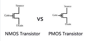
PMOS transistors are often drawn with a small circle at the gate. From the SRAM cell, we can see that M2 an M4 are PMOS transistors, while the other 4 are NMOS transistors.
M1/M2 and M3/M4 are arranged in the form of a CMOS (complementary MOS) inverter.
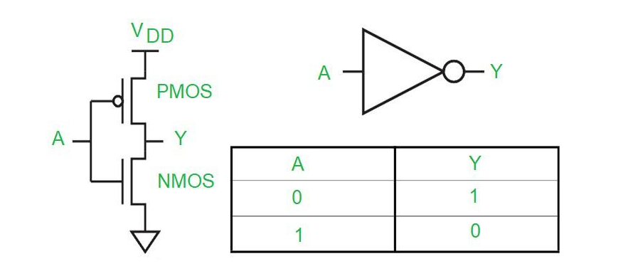
The source of the PMOS (top) is connected to Vdd, while the source of the NMOS (bottom) is connected to ground. The two transistors share a common input voltage and their drains are connected together as well.
When a positive input voltage is applied, the PMOS is off and the NMOS is on, allowing the current to flow from the drain to ground, pulling the output low
When no input voltage is applied, the PMOS is on and NMOS is off, allowing current to flow from Vdd to the common drain, pulling the output high
We can see that M1 and M2 form one CMOS inverter and M3M4 forms another. The output of one inverter is connected to the input of the other, and vice-versa. This forms a cross-coupled inverter, which is also called a bistable latch.
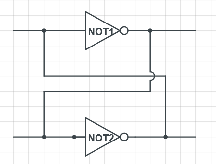
This circuit has two stable states. When the input of inverter 1 is '1', the output of inverter '1' is '0'. This '0' ends up being the input of inverter 2, which outputs '0'. This '0' becomes the input of inverter 1, creating a feedback mechanism that maintains the state of the latch. Thus, when the SRAM cell is not being accessed, the cross-coupled inverters hold their state indefinitely.
With knowledge of how transistors are built to form inverters and latches, we can proceed to analyze how to to read and write from the SRAM cell.
Reading from the SRAM cell The bit line and bit line bar serve as sensing lines to detect the state of the SRAM cell.
Before the read operation, both BL and BL-bar are precharged to a high voltage, near Vdd
The word line is activated, turning on the access transistors M5 and M6
M5 is connected to the input of M3M4 and output of M1M2. M6 is connected to the input of M1M2 and output of M3M4.
Lets assume that the current state of M1M2 is 0 and M3M4 is 1.
This means that transistor M1 is in an on state, allowing a path to flow to ground. Since M5 is also on, bit-line bar gets pulled low.
Now, lets assume the latch is in the other possible state: M1M2 is 1, and M3M4 is 0.
- This means that transistor M3 is in an on state, allowing a path to flow to ground. Since M6 is also on, the bit line gets pulled low. By convention, this means that the output of the M3M4 inverter is the output of the SRAM cell. Nevertheless, both BL and BL-bar are used during read operations. Typically a sense amplifier is used to detect the voltage difference between the two lines because it's easier to detect a difference between two lines than to sense an absolute value on one line. This is called differential sensing, and it also improves noise margins and read speed, because a small difference between the two lines can quickly be amplified to a full logic level.
Writing to the SRAM cell BL and BL-bar are also used to set the state of the SRAM cell.
To store a '1' in the cell, the bit line is driven high and bit line bar is driven low
The word line (WL) is activated. The WL now applies voltage to the gates of M5 and M6, turning them on
The '1' from BL gets applied to the input of the M1M2 inverter and '0' from BL-bar gets applied to the input of the M3M4 inverter.
The M1M2 inverter outputs a '0', which also gets applied to the input of the M3M4 inverter.
The M3M4 inverter outputs a '1', which also gets applied to the input of the M1M2 inverter.
The latch is now in a stable state and a '1' has been stored in the cell.
The same logic applies but in reverse if we want to store a '0' in the cell - BL needs to be driven low and BL-bar driven high, and then the word line needs to be activated.
Summary
Overall, this was a fun exercise and refresher in understanding how transistors are used as fundamental building blocks in digital circuits. We went through how an SRAM circuit is able to hold its state indefinitely (as long as power is constantly provided), as well as how the bit lines are used to read and write from the circuit. This was done by understanding the principles of complementary transistors where NMOS and PMOS transistors work in tandem to create inverters, that when cross coupled form a bistable latch.